Elon Musk and linguists say that AI is forcing us to confront the limits of human language

In analytic philosophy, any meaning can be expressed in language. In his book Expression and Meaning (1979), UC Berkeley philosopher John Searle calls this idea “the principle of expressibility, the principle that whatever can be meant can be said”. Moreover, in the Tractatus Logico-Philosophicus (1921), Ludwig Wittgenstein suggests that “the limits of my language mean the limits of my world”.

Outside the hermetically sealed field of analytic philosophy, the limits of natural language when it comes to meaning-making have long been recognized in both the arts and sciences. Psychology and linguistics acknowledge that language is not a perfect medium. It is generally accepted that much of our thought is non-verbal, and at least some of it might be inexpressible in language. Notably, language often cannot express the concrete experiences engendered by contemporary art and fails to formulate the kind of abstract thought characteristic of much modern science. Language is not a flawless vehicle for conveying thought and feelings.

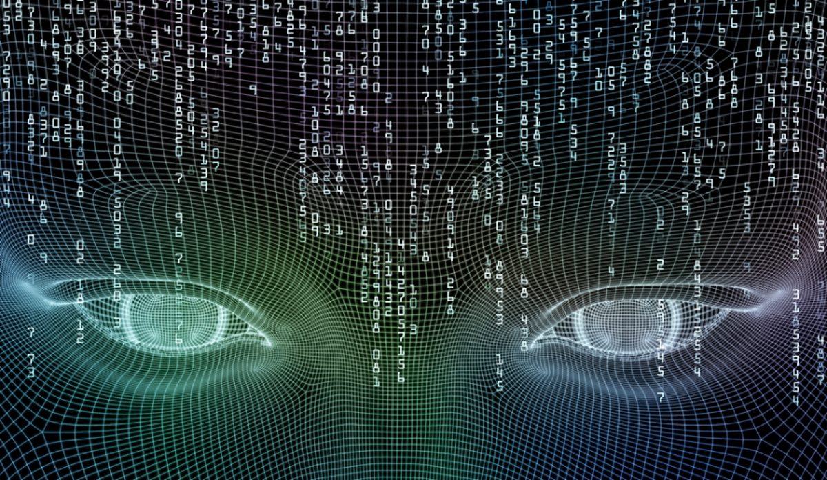
In the field of artificial intelligence, technology can be incomprehensible even to experts. In the essay “Is Artificial Intelligence Permanently Inscrutable?” Princeton neuroscientist Aaron Bornstein discusses this problem with regard to artificial neural networks (computational models): “Nobody knows quite how they work. And that means no one can predict when they might fail.” This could harm people if, for example, doctors relied on this technology to assess whether patients might develop complications.

 The mind is a limitation for artificial intelligence. Bornstein says organizations sometimes choose less efficient but more transparent tools for data analysis and “even governments are starting to show concern about the increasing influence of inscrutable neural-network oracles.” He suggests that “the requirement for interpretability can be seen as another set of constraints, preventing a model from a ‘pure’ solution that pays attention only to the input and output data it is given, and potentially reducing accuracy.” The mind is a limitation for artificial intelligence: “Interpretability could keep such models from reaching their full potential.” Since the work of such technology cannot be fully understood, it is virtually impossible to explain in language.

Ryota Kanai, neuroscientist and CEO of Araya, a Tokyo-based startup, acknowledges that “given the complexity of contemporary neural networks, we have trouble discerning how AIs produce decisions, much less translating the process into a language humans can make sense of.” To that end, Kanai and his colleagues are “trying to implement metacognition in neural networks so that they can communicate their internal states.”

Their ambition is to give a voice to the machine: “We want our machines to explain how and why they do what they do.” This form of communication is to be developed by the machines themselves. With this feedback, researchers will serve as translators who can explain to the public decisions made by the machines. As for human language, Kanai refers to it as “the additional difficulty of teaching AIs to express themselves.” (Incidentally, this assumes that computational models have “selves.”) Language is a challenge for artificial intelligence.

 Neuralink will allegedly connect people to the network in which they will exchange thoughts without wasting their time and energy on language. Elon Musk advances the idea ‘”that we should augment the slow, imprecise communication of our voices with a direct brain-to-computer linkup.” He has founded the company Neuralink that will allegedly connect people to the network in which they will exchange thoughts without wasting their time and energy on language. As Christopher Markou, Cambridge PhD candidate at the Faculty of Law describes it in his essay for The Conversation, “it would enable us to share our thoughts, fears, hopes, and anxieties without demeaning ourselves with written or spoken language”.

Tim Urban, blogger and cartoonist at Wait But Why, presents Musk’s vision of thought communication and argues that “when you consider the ‘lost in transmission’ phenomenon that happens with language, you realize how much more effective group thinking would be.” This project makes sinister assumptions: Instead of enhancing verbal communication, Musk suggests abandoning it as an inadequate means of social interaction. People generally appreciate improvement of the communication networks that transmit language, but instead, they are offered a corporate utopian future of techno-telepathy and an eerily dystopian present where language is an impediment to cooperation. It is both ironic and reassuring that such criticism of language can be successfully communicated by language.

In his recent essay “The Kekulé Problem,” American writer Cormac McCarthy discusses the origins of language and is skeptical about its fundamental role in cognition: “Problems, in general, are often well posed in terms of language and language remains a handy tool for explaining them. But the actual process of thinking—in any discipline—is largely an unconscious affair.” He defines the unconscious as “a machine for operating an animal.”

McCarthy regards language as a relatively recent invention and compares it to a virus that rapidly spread among humans about a hundred thousand years ago. His vision of language is unsatisfactory for a number of reasons. First, language is a human faculty developed due to the gradual evolution of communication; it is problematic to conceive of it as a virus or the result of a sudden invention. Second, thought does not need to be unconscious to be non-verbal. Much conscious thought does not rely on language. Finally, humans may be facing problems that are difficult to convey through language. This might be the key challenge for both the arts and sciences in the immediate future.

While language may not be a perfect medium for thought, it is the most important means of communication that makes possible modern societies, institutions, states, and cultures. Its resourcefulness allows humans to establish social relationships and design new forms of cooperation. It is a robust and highly optimized form of communication, developed through gradual change. For thousands of years, language has been a tool for social interaction. This interaction is facing existential threats (authoritarianism, isolationism, conflict) because the subjective experiences (think of the limits of empathy when it comes to migrants) and the knowledge (think of the complexity of global warming) that are engaged in the arts and sciences appear to have gone beyond the expressive power of language.

 Humanity depends on the capacity of language to communicate complex, new ideas and thus integrate them into culture. Humanity depends on the capacity of language to communicate complex, new ideas and thus integrate them into culture. If people fail to understand and discuss emerging global problems, they will not be able to address them in solidarity with one another. In his essay “Our World Outsmarts Us” for Aeon, Robert Burton, the former associate director of the department of neurosciences at the UCSF Medical Center at Mt Zion, highlights this conundrum when he asks: “If we are not up to the cognitive task, how might we be expected to respond?” Individuals alone cannot stop climate change or curb the rising inequality of income distribution. These goals can only be achieved by concerted efforts. To work together, people need language.

In the arts, it is felt that subjective experiences are not always transmittable by language. Artists confront the limits of concrete expression. Scientists, in their turn, understand that language is a crude tool incapable of conveying abstract ideas. Science thus probes the limits of abstract thought. Both the arts and sciences are dissatisfied with verbal communication. To induce wonder, artists may forego language. To obtain knowledge, scientists often leave language behind.

In his aptly titled essay “Science Has Outgrown the Human Mind and Its Limited Capacities,” Ahmed Alkhateeb, a molecular cancer biologist at Harvard Medical School, suggests outsourcing research to artificial intelligence because “human minds simply cannot reconstruct highly complex natural phenomena efficiently enough in the age of big data.” The problem is that language is a tool for the gathering of knowledge and appreciation of beauty by the whole society.

 Both the arts and sciences are dissatisfied with verbal communication. Scientists understand that language is a crude tool incapable of conveying abstract ideas. And to induce wonder, artists may forego language. Abandoning language marginalizes the arts and sciences. Wonder and knowledge become inaccessible for the community at large. When people make decisions about the future, political processes may fail to register what is happening at the forefront of human thought. Without language, the arts and sciences lose cultural significance and political clout: There is less hope for the arts to move people’s hearts and less opportunity for sciences to enlighten the public. With the arts and sciences on the margins, humanity undermines its cultural safeguards. Today’s dominant narratives foreground the progress of science and the democratization of art, but global challenges necessitate an even more active engagement with scientific, moral, and aesthetic dilemmas on the part of humanity. Language is one of the key tools that can realize this ambition.

It is important to strike a balance between pushing the limits of language and using it as a tool to communicate and collaborate. Artists and scientists might approach the public with ideas that cannot be easily understood and yet need to be conveyed by language. In his essay “To Fix the Climate, Tell Better Stories,” Michael Segal, editor in chief at Nautilus, argues that science needs narratives to become culture. He posits that narratives can help humanity solve global problems. This potential is revealed to us if we look at how “indigenous peoples around the world tell myths which contain warning signs for natural disasters.” Today people can construct helpful narratives based on an expert understanding of the world. These stories can relate unfathomable dangers to the frail human body, and language is the best political vehicle for this task.

In his 2017 New York Times bestseller On Tyranny, Yale historian Timothy Snyder, for example, draws from the history of the 20th century to relate the rise of authoritarian regimes to concrete threats to human life, encouraging his readers to stand up to tyranny. He asks them to take responsibility for the face of the world, defend institutions, remember professional ethics, believe in truth, and challenge the status quo. His language is powerful and clear. Such narratives can help address complex social and environmental problems by using human-scale categories of language.

Ultimately, the arts and sciences grasp critically important knowledge and engage significant experiences, but often fail to express them in language. As Wittgenstein says, “whereof one cannot speak, thereof one must be silent.” This silence might lead to dire consequences for humanity. It is crucial to break the silence. The arts and sciences need to talk to the public and to advance language and culture.

__

This article and images was originally posted on [Open Democracy | Quartz] June 14, 2017 at 10:58AM

BY Pavlo Shopin


IBM unveils world’s first 5nm chip


IBM, working with Samsung and GlobalFoundries, has unveiled the world’s first 5nm silicon chip. Beyond the usual power, performance, and density improvement from moving to smaller transistors, the 5nm IBM chip is notable for being one of the first to use horizontal gate-all-around (GAA) transistors, and the first real use of extreme ultraviolet (EUV) lithography.

GAAFETs are the next evolution of tri-gate finFETs: finFETs, which are currently used for most 22nm-and-below chip designs, will probably run out of steam at around 7nm; GAAFETs may go all the way down to 3nm, especially when combined with EUV. No one really knows what comes after 3nm.

2D, 3D, and back to 2D

For the longest time, transistors were mostly fabricated by depositing layers of different materials on top of each other. As these planar 2D transistors got shorter and shorter (i.e. more transistors in the same space), it became increasingly hard to make transistors that actually perform well (i.e. fast switching, low leakage, reliable). Eventually, the channel got so small that the handful of remaining silicon atoms just couldn’t ferry the electricity across the device quickly enough.

FinFETs solve this problem by moving into the third dimension: instead of the channel being a tiny little 2D patch of silicon, a 3D fin juts out from the substrate, allowing for a much larger volume of silicon. Transistors are still getting smaller, though, and the fins are getting thinner. Now chipmakers need to use another type of transistor that provides yet another stay of execution.

Enter GAAFETs, which are kind of 2D, but they build upon the expertise, machines, and techniques that were required for finFETs. There are a few ways of building GAAFETs, but in this case IBM/Samsung/GloFo are talking about horizontal devices. The easiest way to think of these lateral GAAFETs is to take a finFET and turn it through 90 degrees. Thus, instead of the channel being a vertical fin, the channel becomes a horizontal fin—or to put it another way, the fin is now a silicon nanowire (or nanosheet, depending on its width) stretched between the source and drain.

In the case of IBM’s GAAFET, there are actually three nanosheets stacked on top of each other running between the source and drain, with the gate (the bit that turns the channel on and off) filling in all the gaps. As a result, there’s a relatively large volume of gate and channel material—which is what makes the GAAFET reliable, high-performance, and better suited for scaling down even further.

A side-on shot of the completed gate-all-around transistors. Each transistor consists of three nanosheets stacked on top of each other, with the gate material all around them.

Enlarge /

A side-on shot of the completed gate-all-around transistors. Each transistor consists of three nanosheets stacked on top of each other, with the gate material all around them.

Fabrication-wise, GAAFETs are particularly fascinating. Basically, you lay down some alternating stacks of silicon and silicon-germanium (SiGe). Then you carefully remove the SiGe with a new process called atomic layer etching (probably with an Applied Materials Selectra machine), leaving gaps between each of the silicon layers, which are now technically nanosheets. Finally, without letting those nanosheets droop, you fill those gaps with a high-κ gate metal. Filling the gaps is not easy, though IBM has seemingly managed it with atomic layer deposition (ALD) and the right chemistries.

One major advantage of IBM’s 5nm GAAFETs is a significant reduction in patterning complexity. Ever since we crossed the 28nm node, chips have become increasingly expensive to manufacture, due to the added complexity of fabricating ever-smaller features at ever-increasing densities. Patterning is the multi-stage process where the layout of the chip—defining where the nanosheets and other components will eventually be built—is etched using a lithographic process. As features get smaller and more complex, more patterning stages are required, which drives up the cost and time of producing each wafer.

IBM Research’s silicon devices chief, Huiming Bu, says this 5nm chip is the first time that extreme ultraviolet (EUV) lithography has been used for front-end-of-line patterning. EUV has a much narrower wavelength (13.5nm) than current immersion lithography machines (193nm), which in turn can reduce the number of patterning stages. EUV has been waiting in the wings for about 10 years now, always just a few months away from commercial viability. This is the best sign yet that ASML’s EUV tech is finally ready for primetime.

A few possible paths towards 5nm and 3nm transistors. (Top right shows GAA, but with vertical nanowires rather than the horizontal nanosheets discussed here.)

Enlarge /

A few possible paths towards 5nm and 3nm transistors. (Top right shows GAA, but with vertical nanowires rather than the horizontal nanosheets discussed here.)

Applied Materials

So, how good are GAAFETs?

IBM says that, compared to commercial 10nm chips (presumably Samsung’s 10nm process), the new 5nm tech offers a 40 percent performance boost at the same power, or a 75 percent drop in power consumption at the same performance. Density is also through the roof, with IBM claiming it can squeeze up to 30 billion transistors onto a 50-square-millimetre chip (roughly the size of a fingernail), up from 20 billion transistors on a similarly-sized 7nm chip.

GAAFETs don’t necessarily have the 5nm node sewn up, though. As always with the semiconductor industry, chipmakers prefer to tweak existing fabrication processes and transistor designs, rather than spending billions on deploying new, immature tech. Current silicon-germanium FinFETs will probably get us to 7nm, and the use of exotic III-V semiconductors might take the finFET a step further to 5nm.

At some point, though, it probably won’t be worth the time, cost, and complexity of producing ever-smaller transistors and chips. Someone will realise that much larger gains can be had by going properly 3D: stacking dozens of logic dies on top of each other, connected together with through-silicon vias (TSVs). Intel has been looking at chip stacking to mitigate its slow progress towards the 10nm node since at least 2015. Maybe we’ll soon see the fruits of that labour; though I doubt they’ll be cooled with electronic blood just yet.

__

This article and images was originally posted on [Scientific Method – Ars Technica] June 5, 2017 at 02:25AM

by  (UK)


Here’s How We Can Achieve Mass-Produced Quantum Computers

“These emitters are almost perfect.”

Still waiting patiently for quantum computing to bring about the next revolution in digital processing power? We might now be a little closer, with a discovery that could help us build quantum computers at mass scale.

Scientists have refined a technique using diamond defects to store information, adding silicon to make the readouts more accurate and suitable for use in the quantum computers of the future.

To understand how the new process works, you need to go back to the basics of the quantum computing vision: small particles kept in a state of superposition, where they can represent both 1, 0, and a combination of the two at the same time.

These quantum bits, or qubits, can process calculations on a much grander scale than the bits in today’s computer chips, which are stuck representing either 1 or 0 at any one time.

Getting particles in a state of superposition long enough for us to actually make use of them has proved to be a real challenge for scientists, but one potential solution is through the use of diamond as a base material.

The idea is to use tiny atomic defects inside diamonds to store qubits, and then pass around data at high speeds using light – optical circuits rather than electrical circuits.

Diamond-defect qubits rely on a missing carbon atom inside the diamond lattice which is then replaced by an atom of some other element, like nitrogen. The free electrons created by this defect have a magnetic orientation that can be used as a qubit.

So far so good, but our best efforts so far haven’t been accurate enough to be useful, because of the broad spectrum of frequencies in the light emitted – and that’s where the new research comes in.

Scientists added silicon to the qubit creation process, which emits a much narrower band of light, and supplies the precision that quantum computing requires.

At the moment, these silicon qubits don’t keep their superposition as well, but the researchers are hopeful this can be overcome by reducing their temperature to a fraction of a degree above absolute zero.

“The dream scenario in quantum information processing is to make an optical circuit to shuttle photonic qubits and then position a quantum memory wherever you need it,” says one of the team, Dirk Englund from MIT. “We’re almost there with this. These emitters are almost perfect.”

In fact, the researchers produced defects within 50 nanometres of their ideal locations on average, which is about one thousandth the size of a human hair.

Being able to etch defects with this kind of precision means the process of building optical circuits for quantum computers then becomes more straightforward and feasible.

If the team can improve on the promising results so far, diamonds could be the answer to our quantum computing needs: they also naturally emit light in a way that means qubits can be read without having to alter their states.

You still won’t be powering up a quantum laptop anytime soon, but we’re seeing real progress in the study of the materials and techniques that might one day bring this next-generation processing power to the masses.

The research has been published in Nature Communications.

__

This article and images was originally posted on [ScienceAlert] May 30, 2017 at 06:19PM

By DAVID NIELD

Scientists Claim to Have Invented The World’s First Quantum-Proof Blockchain

Unhackable Bitcoin, anyone?

Researchers in Russia say they’ve developed and tested the world’s first blockchain that won’t be vulnerable to encryption-breaking attacks from future quantum computers.

If the claims are verified, the technique could be a means of protecting the vast amounts of wealth invested in fast-growing cryptocurrencies like Bitcoin and Ethereum– which are safe from today’s code-breaking methods, but could be exposed by tomorrow’s vastly more powerful quantum machines.

A team from the Russian Quantum Centre in Moscow says its quantum blockchain technology has been successfully tested with one of Russia’s largest banks, Gazprombank, and could be used as a proof of concept to underpin secure data encryption and storage methods in the future.

To backtrack a little, a blockchain is a publicly accessible, decentralised ledger of recorded information, spread across multiple computers on the internet.

This kind of distributed database is the underlying technology that makes Bitcoin possible – where it maintains a list of timestamped digital transactions that can be viewed by anyone on the platform.

The idea is that the blockchain frees users on the network from needing any kind of middleman or central authority to regulate transactions or exchanges of information.

Because all interactions are recorded in the distributed ledger, the blockchain makes everything a matter of public record, which, when it comes to Bitcoin, is what ensures that transactions are legitimate, and that units of the currency aren’t duplicated.

The problem with this is that when someone’s computer conducts transactions, the system uses digital signatures for authentication purposes – but while that protection layer may offer strong enough encryption to secure those exchanges today, they won’t be able to withstand quantum computers.

Quantum computers are a technology that’s still in development, but once they mature, they’re set to offer computational power and speed far in excess of what today’s computers can achieve.

While that means quantum computers are poised to do great things for us in tomorrow’s world, it’s a double-edged sword – because that massive increase in performance also means these machines could pose a huge security risk in the world of IT, breaking through comparatively weak encryption walls that currently protect the world of banking, defence, email, social media, you name it.

“If quantum computing takes three decades to truly arrive, there’s no reason to panic,” as Nicole Kobie reported for Wired last year.

“If it lands in 10 years, our data is in serious trouble. But it’s impossible to predict with certainty when it will happen.”

Because of this, today’s security researchers are busy trying to invent secure systems that can defend us from the unbelievably fast supercomputers of tomorrow – a pretty tall order, considering these awesome systems haven’t even really been invented yet.

That’s what the Russian team’s quantum-proof blockchain is – another attempt to devise a digital fortress that won’t be crushed by quantum computers. And the key, the researchers say, is abandoning part of what currently helps protect blockchain transactions.

“In our quantum-secure blockchain setup, we get rid of digital signatures altogether,” one of the researchers, Alexander Lvovsky, told Mary-Ann Russon at IBTimes UK.

“Instead, we utilise quantum cryptography for authentication.”

Quantum cryptography depends on entangled particles to work, and the researchers’ system used what’s called quantum key distribution, which the researchers say makes it possible to make sure nobody’s eavesdropping on private communications.

“Parties that communicate via a quantum channel can be completely sure that they are talking to each other, not anybody else. This is the main idea,” Lvovsky said.

“Then we had to re-invent the entire blockchain architecture to ‘fit’ our new authentication technology, thereby making this architecture immune to quantum computer attacks.”

The system they’ve experimented with was tested on a 3-node (computer) network, but it’s worth pointing out that while the team is claiming victory so far, this kind of research remains hypothetical at this point, and the study has yet to undergo peer-review.

But given the looming technological avalanche that quantum computers represent for digital security, all we’ll say is we’re glad scientists are working on this while there’s still time.

Because, make no doubt, the future is headed this way fast.

The study has been published on pre-print website arXiv.org.

__

This article and images was originally posted on [ScienceAlert] May 30, 2017 at 05:19PM

by PETER DOCKRILL


Google’s latest platform play is artificial intelligence, and it’s already winning

Google has always used its annual I/O conference to connect to developers in its sprawling empire. It announces new tools and initiatives, sprinkles in a little hype, and then tells those watching: choose us, and together we’ll go far. But while in previous years this message has been directed at coders working with Android and Chrome — the world’s biggest mobile OS and web browser respectively — yesterday, CEO Sundar Pichai made it clear that the next platform the company wants to dominate could be even bigger: artificial intelligence.

For Google, this doesn’t just mean using AI to improve its own products. (Although it’s certainly doing that). The company wants individuals and small companies around the world to also get on board. It wants to wield influence in the wider AI ecosystem, and to do so has put together an impressive stack of machine learning tools — from software to servers — that mean you can build an AI product from the ground up without ever leaving the Google playpen.

The heart of this offering is Google’s machine learning software TensorFlow. For building AI tools, it’s like the difference between a command line interface and a modern desktop OS; giving users an accessible framework for grappling with their algorithms. It started life as an in-house tool for the company’s engineers to design and train AI algorithms, but in 2015 was made available for anyone to use as open-source software. Since then, it’s been embraced by the AI community (it’s the most popular software of its type on code repository Github), and is used to create custom tools for a whole range of industries, from aerospace to bioengineering.

“There’s hardly a way around TensorFlow these days,” says Samim Winiger, head of machine learning design studio Samim.io. “I use a lot of open source learning libraries, but there’s been a major shift to TensorFlow.”


One of Google’s server stacks containing its custom TPU machine learning chips.
Photo: Google


Google has made strategic moves to ensure the software is widely used. Earlier this year, for example, it added support for Keras, another popular deep learning framework. According to calculations by the creator of Keras, François Chollet (himself now a Google engineer), TensorFlow was the fastest growing deep learning framework as of September 2016, with Keras in second place. Winiger describes the integration of the two as a “classic tale of Google and how they do it.” He says: “It’s another way that making sure that the entire community converges on their tooling.”

But TensorFlow is also popular for one particularly important reason: it’s good at what it does. “With TensorFlow you get something that scales quickly, works quickly,” James Donkin, a technology manager at UK-based online supermarket Ocado, tells The Verge. He says his team uses a range of machine learning frameworks to create in-house tools for tasks like categorizing customer feedback, but that TensorFlow is often a good place to start. “You get 80 percent of the benefit, and then you might decide to specialize more with other platforms.”

Google offers TensorFlow for free, but it connects easily with the company’s servers for providing data storage or computing power. (“If you use the TensorFlow library it means you can push [products] to Google’s cloud more easily,” says Donkin.) The search giant has even created its own AI-specific chips to power these operations, unveiling the latest iteration of this hardware at this year’s I/O. And, if you want to skip the task of building your own AI algorithms all together, you can buy off-the-shelf components from Google for core tasks like speech transcription and object recognition.

These products and services aren’t necessarily money-makers in themselves, but they other, subtler benefits. They attract talent to Google and help make the company’s in-house software the standard for machine learning. Winiger says these initiatives have helped Google “grab mindshare and make the company’s name synonymous with machine learning.”

Other firms like Amazon, Facebook, and Microsoft also offer their own AI tools, but it’s Google’s that feel pre-eminent. Winiger thinks this is partly down to the company’s capacity to shape the media narrative, but also because of the strong level of support it provides to its users. “There are technical differences between [different AI frameworks], but machine learning communities live off community support and forums, and in that regard Google is winning,” he tells The Verge.

This influence isn’t just abstract, either: it feeds back into Google’s own products. Yesterday, for example, Google announced that Android now has a staggering two billion monthly active users, and to keep the software’s edge, the company is honing it with machine learning. New additions to the OS span the range from tiny tweaks (like smarter text selection) to big new features (like a camera that recognizes what it’s looking at).

But Google didn’t forget to feed the community either, and to complement these announcements unveiled new tools to help developers build AI services that work better on mobile devices. These include a new version of TensorFlow named TensorFlowLite, and an API that will interface with future smartphone chips that have been optimized to work with AI software. Developers can then use these to make better machine learning products for Android devices. Google’s AI empire stretches out a bit further, and Google reaps the benefits.

__

This article and images was originally posted on [The Verge] May 18, 2017 at 06:36AM

by


Using graphene to create quantum bits

Using graphene to create quantum bits

An insulating boron nitride sandwiched between two graphene sheets. Credit: ©EPFL/ LPQM

In the race to produce a quantum computer, a number of projects are seeking a way to create quantum bits—or qubits—that are stable, meaning they are not much affected by changes in their environment. This normally needs highly nonlinear non-dissipative elements capable of functioning at very low temperatures.

In pursuit of this goal, researchers at EPFL’s Laboratory of Photonics and Quantum Measurements LPQM (STI/SB), have investigated a nonlinear graphene-based quantum capacitor, compatible with cryogenic conditions of superconducting circuits, and based on two-dimensional (2D) materials. When connected to a circuit, this capacitor has the potential to produce stable qubits and also offers other advantages, such as being relatively easier to fabricate than many other known nonlinear cryogenic devices, and being much less sensitive to . This research was published in 2D Materials and Applications.


Normal digital computers operate on the basis of a binary code composed of bits with a value of either 0 or 1. In quantum computers, the bits are replaced by qubits, which can be in two states simultaneously, with arbitrary superposition. This significantly boosts their calculation and storage capacity for certain classes of applications. But making qubits is no mean feat: quantum phenomena require highly controlled conditions, including very .


To produce stable qubits, one promising approach is to use superconducting circuits, most of which operate on the basis of the Josephson effect. Unfortunately, they are difficult to make and sensitive to perturbing stray magnetic fields. This means the ultimate circuit must be extremely well shielded both thermally and electromagnetically, which precludes compact integration.


At EPFL’s LPQM, this idea of a capacitor that’s easy to make, less bulky and less prone to interference has been explored. It consists of insulating boron nitride sandwiched between two graphene sheets. Thanks to this sandwich structure and graphene’s unusual properties, the incoming charge is not proportional to the voltage that is generated. This nonlinearity is a necessary step in the process of generating quantum bits. This device could significantly improve the way information is processed but there are also other potential applications too. It could be used to create very nonlinear high-frequency —all the way up to the terahertz regime—or for mixers, amplifiers, and ultra strong coupling between photons.


Explore further:
Refrigerator for quantum computers discovered

__

This article and images was originally posted on [Phys.org – latest science and technology news stories] May 17, 2017 at 10:06PM


A Teenager Just Built The World’s Lightest Satellite – And NASA’s Launching It

Image result

What a legend.

An Indian teenager has won an international competition to build a functioning satellite, and not only has he produced what is reportedly the world’s lightest satellite device – NASA has also agreed to launch it next month.

The tiny satellite weighs just 64 grams (0.14 lb), and will embark on a 4-hour sub-orbital mission launched from NASA’s Wallops Flight Facility in Virginia on June 21. Once positioned in microgravity, its main objective will be to test the durability of its extremely light, 3D-printed casing.

“We designed it completely from scratch,” 18-year-old Rifath Shaarook told Business Standard.

“It will have a new kind of on-board computer and eight … built-in sensors to measure acceleration, rotation, and the magnetosphere of Earth.”

Shaarook entered his invention into the Cubes in Space competition, run by education company idoodlelearning, and supported by NASA and the Colorado Space Grant Consortium.

The challenge presented to school students was to invent a device that could fit into a 4-metre (13-foot) cube, and weigh no more than 64 grams. And, most importantly, it had to be space-worthy.

The tiny satellite that topped all the entries has been named KalamSat, after Indian nuclear scientist and former President, A.P.J. Abdul Kalam.

It owes its lightness to its reinforced carbon fibre polymer frame – a material that has a super-high strength-to-weight ratio, and is used in everything from aerospace engineering to fishing line.

On June 21, it will be launched into sub-orbital flight, where it will complete a 4-hour round trip, and be online and operational for 12 minutes in the micro-gravity environment of space. (Sub-orbital means it goes up and comes back down, whereas orbital means it will continue circling the globe.)

NASA has made a habit out of seeking ideas from outside its expert cohort of scientists and engineers, proving that it doesn’t matter who you are – or how young – good science can come from anywhere.

Back in March, the space agency made headlines when its data was corrected by a 17-year-old student in the UK.

The teen, Miles Soloman, had been studying data recorded by radiation detectors on the International Space Station (ISS) during British astronaut Tim Peake’s six-month stay, and noticed an error in the reported energy levels.

And just weeks ago, NASA also announced that it would be launching a device called the miniPCR to the ISS to test space-faring microbes in situ for the first time ever. That device was also invented by a teen – a 17-year-old student named Anna-Sophia Boguraev.

We can’t wait to see where these amazing role models go next – and good luck to Rifath Shaarook on his launch next month!

__

This article and images was originally posted on [ScienceAlert] May 16, 2017 at 06:21PM

by BEC CREW


Cybersecurity Pros Will Soon Patrol Computer Networks Like Agents in ‘The Matrix’

Security analysts could soon become the first employees asked to show up to work inside virtual reality.

Thanks to a new virtual reality tool built by the Colorado-based startup ProtectWise, cyMrbnb091984

bersecurity professionals may soon be patrolling computer networks — like real world beat cops — inside a three-dimensional video game world.

Scott Chasin, CEO and co-founder of ProtectWise, sees a future in which companies might even have war-rooms of Oculus Rift-wearing security analysts who patrol their networks in VR. “I see an opportunity in the not-too-distant future in which a large organization who has a lot of IT infrastructure might have rooms full of security analysts with augmented reality and VR headsets on,” he told me.

Their ProtectWise Grid product is launching a virtual reality user interface tool called Immersive Grid where each connected asset in a company — a server, PC, mobile device, whatever — is represented as a building inside a virtual city. A company can group those device-buildings into neighborhoods or zones — organized by business unit or geography. For example, the marketing department might have their devices located in one part of the city while the London office’s are grouped in another.

The analysts can then monitor and patrol those buildings, which convey information about data traffic and security threats related to that device. The shape of the building — perhaps it’s round or square — designates what type of device it is; the height represents the IP network traffic; and the width indicates how much bandwidth is going to the device. If a building turns red or orange, an analyst would know there’s an elevated level of risk or unusual activity associated with that particular asset.

Chasin hopes visualization technology like this might transform the technically complicated work of a security analyst into something more like playing a video game.

That could widen the pool for who is a good fit for the job and reduce the technical-skill barrier preventing people from getting into the profession. Today, there’s a major shortage of qualified cybersecurity professionals — a talent gap that’s expected to grow — and the reason, according to Chasin, is the knowledge base required for the job is fairly large.

“Today, you have to work with terminal windows, shell-scripts, python scripts, and have an understanding of forensic analysis. Using visual filtering techniques — someone without any experience in shell-script or python can see everything at once,” Chasin says.

Chasin also points out that a younger generation of employees might be well-suited for the interface.

“We see an opportunity to tap into that next generation, the Minecraft generation, that can reason about data visually. There’s now a younger generation who understand virtual worlds and the mechanics of games with a skill-set that’s suited to a platform like Immersive Grid.”

All this almost sounds like a vision straight from science fiction — like Neuromancer, where hackers prowl the virtual reality “cyberspace” for corporate and military targets, or Ender’s Game, where a youthful, games-savvy generation are used to create real-world consequences through their gameplay. As society continues to see explosive growth in the popularity of eSports and a cultural shift towards valuing competitive video games, we’re even now seeing gaming find a place inside big-name collegiate sports programs.

If visual interfaces like Immersive Grid become more common, those gaming skills might actually translate into the business world.

Chasin believes this type of interface will have a real world impact on the way security is managed in the future. “We’re talking about a technology set that will allow us to actually build cyberspace,” he says.

And what he’s talking about may have an impact beyond cybersecurity. The influence of 3D interfaces on the way humans interact with the digital world will bring about a shift as dramatic as moving from text to graphical user interfaces. Humans are natively 3D thinkers, so moving to augmented and virtual worlds to interact with data could accelerate the human ability to manage our world.

It might sound like some far-off scenario pulled from science fiction, but sooner than we think, significant numbers of people may be showing up to work inside a virtual reality headset device.

Image Credit: ProtectWise

__

This article and images was originally posted on [Singularity Hub] May 8, 2017 at 04:05AM

Drug Discovery AI Can Do in a Day What Currently Takes Months

To create a new drug, researchers have to test tens of thousands of compounds to determine how they interact. And that’s the easy part; after a substance is found to be effective against a disease, it has to perform well in three different phases of clinical trials and be approved by regulatory bodies.

It’s estimated that, on average, one new drug coming to market can take 1,000 people, 12-15 years, and up to $1.6 billion.

There has to be a better way—and now it seems there is.

Last week, researchers published a paper detailing an artificial intelligence system made to help discover new drugs, and significantly shorten the amount of time and money it takes to do so.

The system is called AtomNet, and it comes from San Francisco-based startup AtomWise. The technology aims to streamline the initial phase of drug discovery, which involves analyzing how different molecules interact with one another—specifically, scientists need to determine which molecules will bind together and how strongly. They use trial and error and process of elimination to analyze tens of thousands of compounds, both natural and synthetic.

AtomNet takes the legwork out of this process, using deep learning to predict how molecules will behave and how likely they are to bind together. The software teaches itself about molecular interaction by identifying patterns, similar to how AI learns to recognize images.

Remember the 3D models of atoms you made in high school, where you used pipe cleaners and foam balls to represent the connections between protons, neutrons and electrons? AtomNet uses similar digital 3D models of molecules, incorporating data about their structure to predict their bioactivity.

As AtomWise COO Alexander Levy put it, “You can take an interaction between a drug and huge biological system and you can decompose that to smaller and smaller interactive groups. If you study enough historical examples of molecules…you can then make predictions that are extremely accurate yet also extremely fast.”

“Fast” may even be an understatement; AtomNet can reportedly screen one million compounds in a day, a volume that would take months via traditional methods.

AtomNet can’t actually invent a new drug, or even say for sure whether a combination of two molecules will yield an effective drug. What it can do is predict how likely a compound is to work against a certain illness. Researchers then use those predictions to narrow thousands of options down to dozens (or less), focusing their testing where there’s more likely to be positive results.

The software has already proven itself by helping create new drugs for two diseases, Ebola and multiple sclerosis. The MS drug has been licensed to a British pharmaceutical company, and the Ebola drug is being submitted to a peer-reviewed journal for additional analysis.

While AtomNet is a promising technology that will make discovering new drugs faster and easier, it’s worth noting that the future of medicine is also moving towards a proactive rather than reactive approach; rather than solely inventing drugs to cure sick people, focus will shift to carefully monitoring our health and taking necessary steps to keep us from getting sick in the first place.

Last year, the Chan Zuckerberg Initiative donated $3 billion in a pledge to “cure all diseases.” It’s an ambitious and somewhat quixotic goal, but admirable nonetheless. In another example of the movement towards proactive healthcare, the XPRIZE foundation recently awarded $2.5 million for a device meant to facilitate home-based diagnostics and personal health monitoring. Proactive healthcare technology is likely to keep advancing and growing in popularity.

That doesn’t mean reactive healthcare shouldn’t advance alongside it; fifty or one hundred years from now, people will still be getting sick and will still need medicine to help cure them. AtomNet is the first software of its kind, and it may soon see others following in its footsteps in the effort to apply AI to large-scale challenges.

Image Credit: Shutterstock

__

This article and images was originally posted on [Singularity Hub] May 7, 2017 at 04:01AM

Quantum Computing Demands a Whole New Kind of Programmer

Quantum computers finally seem to be coming of age with promises of “quantum supremacy” by the end of the year. But there’s a problem—very few people know how to work them.

The bold claim of achieving “quantum supremacy” came on the back of Google unveiling a new quantum chip design. The hyperbolic phrase essentially means building a quantum device that can perform a calculation impossible for any conventional computer.

In theory, quantum computers can crush conventional ones at important tasks like factoring large numbers. That’s because unlike normal computers, whose bits can either be represented as 0 or 1, a quantum bit—or “qubit”—can be simultaneously 0 and 1 thanks to a phenomenon known as superposition.

Demonstrating this would require thousands of qubits, though, which is well beyond current capabilities. So instead Google plans to compare the computers’ ability to simulate the behavior of a random arrangement of quantum circuits. They predict it should take 50 qubits to outdo the most powerful supercomputers, a goal they feel they can reach this year.

Clearly the nature of the experiment tips the balance in favor of their chip, but the result would be impressive nonetheless, and could act as a catalyst to spur commercialization of the technology.

This year should also see the first commercial ‘universal’ quantum computing service go live, with IBM giving customers access to one of its quantum computers over the cloud for a fee. Canadian company D-Wave already provides cloud access to one of its machines, but its quantum computers are not universal, as they can only solve certain optimization problems.

But despite this apparent impetus, the technology has a major challenge to overcome. Programming these devices is much harder than programming conventional computers.

For a start, building algorithms for these machines requires a certain level of understanding about the quantum physics that gives qubits their special properties. While you don’t need an advanced physics degree to get your head around it, it is a big departure from traditional computer programming.

Writing in ReadWrite, Dan Rowinski points out, “Writing apps that can be translated into some form of qubit-relatable code may require some very different approaches, since among other things, the underlying logic for digital programs may not translate precisely (or at all) to the quantum-computing realm.”

And while there are a number of quantum simulators that can run on a laptop for those who want to dip their toes in the water, real quantum computers are likely to behave quite differently. “The real challenge is whether you can make your algorithm work on real hardware that has imperfections,” Isaac Chuang, an MIT physicist, told Nature.

Convincing programmers to invest the time necessary to learn these skills is going to be tricky until commercial systems are delivering tangible benefits and securing customers, but that’s going to be tough if there’s no software to run on them.

The companies building these machines recognize this chicken and egg problem, and it is why there is an increasing drive to broaden access to these machines. Before the announcement of the commercial IBMQ service, the company had already released the free Quantum Experience service last year.

Earlier this year, D-Wave open sourced their Qbsolv and Qmasm tools to allow people to start getting to grips with programming its devices, while a pair of Google engineers built a “Quantum Computing Playground” for people to start investigating the basics of the technology. The company plans to provide access to its devices over the cloud just like IBM.

“We don’t just want to build these machines,” Jerry Chow, the manager of IBM’s Experimental Quantum Computing team told Wired. “We want to build a framework that allows people to use them.”

How easy it will be to translate the skills learned in one of these companies’ proprietary quantum computing ecosystems to another also remains to be seen, not least because the technology at the heart of them can be dramatically different. This could be a further stumbling block to developing a solid pool of quantum programmers.

Ultimately, the kinds of large-scale quantum computers powerful enough to be usefully put to work on real-world problems are still some years away, so there’s no need to panic yet. But as the researchers behind Google’s quantum effort note in an article in Nature, this scarcity of programming talent also presents an opportunity for those who move quickly.

“If early quantum-computing devices can offer even a modest increase in computing speed or power, early adopters will reap the rewards,” they write. “Rival companies would face high entry barriers to match the same quality of services and products, because few experts can write quantum algorithms, and businesses need time to tailor new algorithms.”

Image Credit: Shutterstock

__

This article and images was originally posted on [Singularity Hub] May 9, 2017 at 04:02AM

by Edd Gent


Neil deGrasse Tyson Warns Science Denial Could ‘Dismantle’ Democracy

Neil deGrasse Tyson says that when people who deny science rise to power that is a recipe for a complete dismantling of our democracy.

Credit: Redglass Pictures/YouTube

Renowned astrophysicist Neil deGrasse Tyson urges Americans to become more scientifically literate in a short video he posted yesterday (April 19) on his Facebook page.

 
In the video he titled “Science in America,” Tyson comments on 21st-century attitudes toward science, explaining the importance of the scientific method and making the case that science denial could erode democracy.

 
“Dear Facebook Universe,” he wrote. “I offer this four-minute video on ‘Science in America’ containing what may be the most important words I have ever spoken. As always, but especially these days, keep looking up.” [2017 March for Science: What You Need to Know]


Tyson, who is the director of the Hayden Planetarium in New York City, the author of several books and a star of TV and radio, has been speaking for years against the troubling decline of basic science knowledge in America.

 
The video begins with a reminder that the United States rose up from a “backwoods country,” as Tysoncalls it, to “one of the greatest nations the world has ever known,” thanks to science. It was the United States that put humans on the moon and whose big thinkers created the personal computer and the internet.

 
“We pioneered industries,” Tysonsaid. “Science is a fundamental part of the country that we are.”

 
But in the 21st century, a disturbing trend took hold: “People have lost the ability to judge what is true and what is not,” he said.

 
In a voice full of passion, Tyson said, “This is science,” as images flash across the screen showing the world’s great scientists from Albert Einstein to Jane Goodall, and scientific accomplishments, from ultrasound images of a fetus and robotic surgery to animations of solar flares and pictures of a swirling hurricane.

 
“It’s not something to say ‘I choose not to believe E = mc^2,’ you don’t have that option.”

 
Tyson points to scientific issues that have become highly controversial: vaccinations, human-caused climate change, genetically modified foods, even evolution. One clip shows Vice President Mike Pence, then a congressman, saying, “Let us demand that educators around America teach evolution not as fact, but as theory.” (Evolution is a scientific fact; so much so that the evidence supporting its occurrence is undeniable, according to the National Academy of Sciences.)

 
Tyson suggests that those who understand science the least are the people who are rising to power and denying it the loudest.

 
“That is a recipe for the complete dismantling of our informed democracy,” he said.

 
In about 30 seconds, Tyson explains how hypothesis and experimentation, fundamental ingredients of the scientific method, lead to emergent truths. “The scientific method does it better than anything else we have ever done as human beings,” he said.

 
Emergent scientific truths are true whether or not a person believes them, he said. “And the sooner you understand that, the faster we can get on with the political conversations about how to solve the problems that face us.”

 
Every minute a person is in denial only delays the political solution, he said. Tyson wants voters and citizens to learn what science is and how it works to make more informed decisions.

 
“It’s in our hands,” he said.

 
Original article on Live Science.


__

Join our fans by liking us on Facebook, or follow us on Twitter, Google+, feedly, flipboardand Instagram.

This article and images was originally posted on Live Science

By Tracy Staedter, Live Science Contributor


Rechargeable ‘spin battery’ promising for spintronics and quantum computing

Rechargeable ‘spin battery’ promising for spintronics and quantum computing
This microscope image shows a new device used to measure the “persistent spin polarization” for a rechargeable “spin battery” that represents a step toward building possible spintronic devices and quantum computers more powerful than today’s technologies. Credit: Purdue University image/Jifa Tian

Researchers have shown how to create a rechargeable “spin battery” made out of materials called topological insulators, a step toward building new spintronic devices and quantum computers.

Unlike ordinary that are either insulators or conductors, topological insulators are both at the same time – they are insulators inside but conduct electricity on the surface. The materials might be used for spintronic devices and quantum computers more powerful than today’s technologies.

Electrons can be thought of as having two : up or down, and a phenomenon known as superposition allows electrons to be in both states at the same time. Such a property could be harnessed to perform calculations using the laws of quantum mechanics, making for computers much faster than conventional computers at certain tasks.

The conducting electrons on the surface of topological insulators have a key property known as “spin momentum locking,” in which the direction of the motion of electrons determines the direction of its spin. This spin could be used to encode or carry information by using the down or up directions to represent 0 or 1 for spin-based information processing and computing, or spintronics.

“Because of the spin-momentum locking, you can make the spin of electrons line up or ‘locked’ in one direction if you pass a current through the topological insulator material, and this is a very interesting effect,” said Yong P. Chen, a Purdue University professor of physics and astronomy and electrical and computer engineering and director of the Purdue Quantum Center.

Applying an electric current to the material induces an electron “spin polarization” that might be used for spintronics. Ordinarily, the current must remain turned on to maintain this polarization. However, in new findings, Purdue researchers are the first to induce a long-lived electron spin polarization lasting two days even when the current is turned off. The is detected by a magnetic voltage probe, which acts as a spin-sensitive voltmeter in a technique known as “spin potentiometry”.

The new findings are detailed in a research paper appearing on April 14 in the journal Science Advances. The experiment was led by postdoctoral research associate Jifa Tian.

“Such an electrically controlled persistent spin polarization with unprecedented long lifetime could enable a rechargeable spin battery and rewritable spin memory for potential applications in spintronics and quantum information systems,” Tian said.

This “writing current” could be likened to recording the ones and zeroes in a computer’s memory.

“However, a better analog is that of a battery,” Chen said. “The writing current is like a charging current. It’s slow, just like charging your iPhone for an hour or two, and then it can output power for several days. That’s the similar idea. We charge up this spin battery using this writing current in half an hour or one hour and then the spins stay polarized for two days, like a rechargeable battery.”

Rechargeable ‘spin battery’ promising for spintronics and quantum computing
This schematic describes a proposed “spin transfer” of electrons to atomic nuclei in materials called topological insulators, a promising step toward building new spintronic devices or quantum computers. Credit: Purdue University image/Jifa Tian

The finding was a surprise.

“This was not predicted nor something we were looking for when we started the experiment,” he said. “It was an accidental discovery, thanks to Jifa’s patience and persistence, running and repeating the measurements many times, and effectively charging up the spin battery to output a measurable persistent signal.”

The researchers are unsure what causes the effect. However, one theory is that the spin- polarized electrons might be transferring their polarization to the atomic nuclei in the material. This hypothesis as a possible explanation to the experiment was proposed by Supriyo Datta, Purdue’s Thomas Duncan Distinguished Professor of Electrical and Computer Engineering and the leader of the recently launched Purdue “spintronics preeminent team initiative.”

“In one meeting, Professor Datta made the critical suggestion that the persistent spin signal Jifa observed looked like a battery,” Chen said. “There were some analogous experiments done earlier on a powered battery, although they typically required much more challenging conditions such as high magnetic fields. Our observation so far is consistent with the effect also arising from the nuclear spins, even though we don’t have direct evidence.”

Nuclear spin has implications for development of quantum memory and quantum computing.

“And now we have an electrical way to achieve this, meaning it is potentially useful for quantum circuits because you can just pass current and you polarize nuclear spin,” Chen said. “Traditionally that has been very difficult to achieve. Our spin battery based on works even at zero magnetic field, and moderately low temperatures such as tens of kelvins, which is very unusual.”

Seokmin Hong, a former Purdue doctoral student working with Datta who is now a software engineer at Intel Corp., said, “While an ordinary charged battery outputs a voltage that can be used to drive a charge current, a ‘spin battery’ outputs a ‘spin voltage,’ or more precisely a chemical potential difference between the spin up and spin down electrons, that can be used to drive a non-equilibrium spin current.”

The researchers used small flakes of a material called bismuth tellurium selenide. It is in the same class of materials as bismuth telluride, which is behind solid-state cooling technologies such as commercial thermoelectric refrigerators. However, unlike the commercial grade material that is a “doped” bulk semiconductor, the material used in the experiment was carefully produced to have ultra-high-purity and little doping in the bulk so the conduction is dominated by the spin-polarized electrons on the surface. It was synthesized by research scientist Ireneusz Miotkowski in the semiconductor bulk crystal lab managed by Chen in Purdue’s Department of Physics and Astronomy. The devices were fabricated by Tian in the Birck Nanotechnology Center in Purdue’s Discovery Park.

The paper was authored by Tian; Hong; and Miotkowski, Datta, and Chen.

Future research will include work to probe what causes the effect by directly probing the nuclear spin, and also to explore how this spin can be used in potential practical applications.

Explore further: Long-distance transport of electron spins for spin-based logic devices

More information: Jifa Tian et al. Observation of current-induced, long-lived persistent spin polarization in a topological insulator: A rechargeable spin battery, Science Advances (2017). DOI: 10.1126/sciadv.1602531

__

Join our fans by liking us on Facebook, or follow us on Twitter, Google+, feedly, flipboardand Instagram.

This article and images was originally posted on Phys.org | Provided by: Purdue University search and more info

by Emil Venere


AI can predict heart attacks more accurately than doctors

An estimated 20 million people die each year due to cardiovascular disease. Luckily, a team of researchers from the University of Nottingham in the UK have developed a machine-learning algorithm that can predict your likelihood of having a heart attack or stroke as well as any doctor.

The American College of Cardiology/American Heart Association (ACC/AHA) has developed a series of guidelines for estimating a patient’s cardiovascular risk which is based on eight factors including age, cholesterol level and blood pressure. On average, this system correctly guesses a person’s risk at a rate of 72.8 percent.

That’s pretty accurate but Stephen Weng and his team set about to make it better. They built four computer learning algorithms, then fed them data from 378,256 patients in the United Kingdom. The systems first used around 295,000 records to generate their internal predictive models. Then they used the remaining records to test and refine them. The algorithms results significantly outperformed the AAA/AHA guidelines, ranging from 74.5 to 76.4 percent accuracy. The neural network algorithm tested highest, beating the existing guidelines by 7.6 percent while raising 1.6 percent fewer false alarms.

Out of the 83,000 patient set of test records, this system could have saved 355 extra lives. Interestingly, the AI systems identified a number of risk factors and predictors not covered in the existing guidelines, like severe mental illness and the consumption of oral corticosteroids. “There’s a lot of interaction in biological systems,” Weng told Science. “That’s the reality of the human body. What computer science allows us to do is to explore those associations.”

Source: Science

__

Join our fans by liking us on Facebook, or follow us on Twitter, Google+, feedly, flipboardand Instagram.

This article and images was originally posted on Engadget

by Andrew Tarantola, @terrortola


Graphene ‘phototransistor’ promising for optical technologies

A graphene field-effect transistor, or GFET, developed at Purdue University could bring high-performance photodetectors for various potential applications. Credit: Purdue University image/Erin Easterling

Researchers have solved a problem hindering development of highly sensitive optical devices made of a material called graphene, an advance that could bring applications from imaging and displays to sensors and high-speed communications.

Graphene is an extremely thin layer of carbon that is promising for optoelectronics, and researchers are trying to develop graphene-based photodetectors, devices that are critical for many technologies. However, typical photodetectors made of graphene have only a small area that is sensitive to light, limiting their performance.

Now, researchers have solved the problem by combining graphene with a comparatively much larger silicon carbide substrate, creating graphene field-effect transistors, or GFETs, which can be activated by light, said Yong Chen, a Purdue University professor of physics and astronomy and electrical and computer engineering, and director of the Purdue Quantum Center.

High-performance photodetectors might be useful for applications including high-speed communications and ultra-sensitive cameras for astrophysics, as well as sensing applications and wearable electronics. Arrays of the graphene-based transistors might bring high-resolution imaging and displays.

“In most cameras you need lots of pixels,” said Igor Jovanovic, a professor of nuclear engineering and radiological sciences at the University of Michigan. “However, our approach could make possible a very sensitive camera where you have relatively few pixels but still have high resolution.”

New findings are detailed in a research paper appearing this week in the journal Nature Nanotechnology. The work was performed by researchers at Purdue, the University of Michigan and Pennsylvania State University.

“In typical graphene-based photodetectors demonstrated so far, the photoresponse only comes from specific locations near graphene over an area much smaller than the device size,” Jovanovic said. “However, for many optoelectronic device applications, it is desirable to obtain photoresponse and positional sensitivity over a much larger area.”

New findings show the device is responsive to light even when the silicon carbide is illuminated at distances far from the graphene. The performance can be increased by as much as 10 times depending on which part of the material is illuminated. The new phototransistor also is “position-sensitive,” meaning it can determine the location from which the light is coming, which is important for imaging applications and for detectors.

“This is the first time anyone has demonstrated the use of a small piece of graphene on a large wafer of silicon carbide to achieve non-local photodetection, so the light doesn’t have to hit the graphene itself,” Chen said. “Here, the light can be incident on a much larger area, almost a millimeter, which has not been done before.”

A voltage is applied between the back side of the silicon carbide and the graphene, setting up an electric field in the silicon carbide. Incoming light generates “photo carriers” in the silicon carbide.

The video will load shortly

Video via: Purdue Engineering

“The semiconductor provides the media that interact with light,” Jovanovic said. “When light comes in, part of the device becomes conducting and that changes the electric field acting on graphene.”

This change in the electric field also changes the conductivity of graphene itself, which is detected. The approach is called field-effect photo detection.

The silicon carbide is “un-doped,” unlike conventional semiconductors in silicon-based transistors. Being un-doped makes the material an insulator unless it is exposed to light, which temporarily causes it to become partially conductive, changing the electric field on the graphene.

“This is a novelty of this work,” Chen said.

The research is related to work to develop new graphene-based sensors designed to detect radiation and was funded with a joint grant from the National Science Foundation and the U.S. Department of Homeland Security and another grant from the Defense Threat Reduction Agency.

“This particular paper is about a sensor to detect photons, but the principles are the same for other types of radiation,” Chen said. “We are using the sensitive transistor to detect the changed caused by photons, light in this case, interacting with a substrate.”

Light detectors can be used in devices called scintillators, which are used to detect radiation. Ionizing radiation creates brief flashes of , which in scintillators are detected by devices called photo multiplier tubes, a roughly century-old technology.

“So there is a lot of interest in developing advanced semiconductor-based devices that can achieve the same function,” Jovanovic said.

The paper was authored by former Purdue postdoctoral research associate Biddut K. Sarker; former Penn State graduate student Edward Cazalas; Purdue graduate student Ting-Fung Chung; former Purdue graduate student Isaac Childres; Jovanovic; and Chen.

The researchers also explained their findings with a computational model. The transistors were fabricated at the Birck Nanotechnology Center in Purdue’s Discovery Park.

Future research will include work to explore applications such as scintillators, imaging technologies for astrophysics and sensors for high-energy radiation.


Explore further:
Researchers ‘iron out’ graphene’s wrinkles

__

Join our fans by liking us on Facebook, or follow us on Twitter, Google+, feedly, flipboardand Instagram.

This article and images was originally posted on Phys.org

Provided by: Purdue University search and more info


OpenAI Just Beat Google DeepMind at Atari With an Algorithm From the 80s

AI research has a long history of repurposing old ideas that have gone out of style. Now researchers at Elon Musk’s open source AI project have revisited “neuroevolution,” a field that has been around since the 1980s, and achieved state-of-the-art results.

The group, led by OpenAI’s research director Ilya Sutskever, has been exploring the use of a subset of algorithms from this field, called “evolution strategies,” which are aimed at solving optimization problems.

Despite the name, the approach is only loosely linked to biological evolution, the researchers say in a blog post announcing their results. On an abstract level, it relies on allowing successful individuals to pass on their characteristics to future generations. The researchers have taken these algorithms and reworked them to work better with deep neural networks and run on large-scale distributed computing systems.

“To validate their effectiveness, they then set them to work on a series of challenges seen as benchmarks for reinforcement learning.”

To validate their effectiveness, they then set them to work on a series of challenges seen as benchmarks for reinforcement learning, the technique behind many of Google DeepMind’s most impressive feats, including beating a champion Go player last year.

One of these challenges is to train the algorithm to play a variety of computer games developed by Atari. DeepMind made the news in 2013 when it showed it could use Deep Q-Learning—a combination of reinforcement learning and convolutional neural networks—to successfully tackle seven such games. The other is to get an algorithm to learn how to control a virtual humanoid walker in a physics engine.

To do this, the algorithm starts with a random policy—the set of rules that govern how the system should behave to get a high score in an Atari game, for example. It then creates several hundred copies of the policy—with some random variation—and these are tested on the game.

These policies are then mixed back together again, but with greater weight given to the policies that got the highest score in the game. The process repeats until the system comes up with a policy that can play the game well.

“In one hour training on the Atari challenge, the algorithm reached a level of mastery that took a [DeepMind] reinforcement-learning system…a whole day to learn.”

In one hour training on the Atari challenge, the algorithm reached a level of mastery that took a reinforcement-learning system published by DeepMind last year a whole day to learn. On the walking problem the system took 10 minutes, compared to 10 hours for Google’s approach.

One of the keys to this dramatic performance was the fact that the approach is highly “parallelizable.” To solve the walking simulation, they spread computations over 1,440 CPU cores, while in the Atari challenge they used 720.

This is possible because it requires limited communication between the various “worker” algorithms testing the candidate policies. Scaling reinforcement algorithms like the one from DeepMind in the same way is challenging because there needs to be much more communication, the researchers say.

The approach also doesn’t require backpropagation, a common technique in neural network-based approaches, including deep reinforcement learning. This effectively compares the network’s output with the desired output and then feeds the resulting information back into the network to help optimize it.

The researchers say this makes the code shorter and the algorithm between two and three times faster in practice. They also suggest it will be particularly suited to longer challenges and situations where actions have long-lasting effects that may not become apparent until many steps down the line.

The approach does have its limitations, though. These kinds of algorithms are usually compared based on their data efficiency—the number of iterations required to achieve a specific score in a game, for example. On this metric, the OpenAI approach does worse than reinforcement learning approaches, although this is offset by the fact that it is highly parallelizable and so can carry out iterations more quickly.

For supervised learning problems like image classification and speech recognition, which currently have the most real-world applications, the approach can also be as much as 1,000 times slower than other approaches that use backpropagation.

Nevertheless, the work demonstrates promising new applications for out-of-style evolutionary approaches, and OpenAI is not the only group investigating them. Google has been experimenting on using similar strategies to devise better image recognition algorithms. Whether this represents the next evolution in AI we will have to wait and see.

Image Credit: Shutterstock

__

Join our fans by liking us on Facebook, or follow us on Twitter, Google+, feedly, flipboardand Instagram.

This article and images was originally posted on Singularity Hub

Massive 3-D Cell Library Teaches Computers How to Find Mitochondria

__

Join our fans by liking us on Facebook, or follow us on Twitter, Google+, feedly, flipboardand Instagram.

This article and images was originally posted on WIRED

By 


How AI Is Like Electricity—and Why That Matters

What’s the first thing that comes to mind when you hear ‘artificial intelligence’? For those raised on a steady diet of big budget Hollywood sci-fi, the answer to that question is something along the lines of “evil robots and all-knowing computers that are going to destroy humanity.”

But AI is already playing an active role in our day-to-day lives, and its capabilities are only going to increase from here on out. To help ease the anxiety that will likely accompany that increase, Wired founding editor Kevin Kelly has suggested we re-frame the way we’re thinking about AI, both by changing the vocabulary we use for it and by putting it into historical context.

Kelly thinks the word ‘intelligence’ has taken on undue baggage, including a somewhat negative connotation. When it’s not used in reference to a human mind, the word can conjure images of spying, classified information, or invasion of privacy.

Since the scope of artificial intelligence goes far beyond that, and we may be past the point of instilling a new definition of old words, why not use new words instead?

Kelly’s word of choice is cognification, and he uses it to describe ‘smart’ things.

At this point only a handful of things have been cognified, and more are in process: phones, cars, thermostats, TVs. But in the future, Kelly says, everything that’s already been electrified will also be cognified. Smart homes? Smart office buildings? Smart cities? Only a matter of time.

The cognification of things can be viewed similarly to the electrification of things that took place during the Industrial Revolution.

The industrial revolution saw a large-scale switch from the agricultural world—where everything that was made was made by muscle power—to the mechanized world, where gasoline, steam engines, and electricity applied artificial power to everything. We made a grid to deliver that power, so we could have it on-demand anytime and anywhere we wanted, and everything that used to require natural power could be done with artificial power.

Movement and transportation, among other things, were amplified by this new power. Kelly gives the example of a car, which is simple but compelling: you summon the power of 250 horses just by turning a key. Pressing your foot to the gas pedal can make your vehicle go 60 miles an hour, which would have been unthinkable in the era when all we had to go off of was muscle power.

The next step is to take that same car that already has the artificial power of 250 horses and add the power of 250 artificial minds. The result? Self-driving cars that can not only go fast, they can make decisions and judgment calls, deliver us to our destinations, and lower the risk of fatal accidents.

According to Kelly, we’re currently in the dawn of another industrial revolution. As it progresses, we’ll take everything we’ve previously electrified, and we’ll cognify it.

Imagining life before the Industrial Revolution, we mostly wonder how we ever lived without electricity and human-made power, thinking, “Wow, I’m sure glad we have lights and airplanes and email now. It’s nice not to have to light candles, ride in covered wagons, or send handwritten letters.” Admittedly, our relief is sometimes mixed with some nostalgia for those simpler times.

What will people think in 200 years? Once everything has been cognified and the world is one big smart bubble, people will probably have some nostalgia for the current ‘simpler times’—but they’ll also look back and say, “How did we ever live without ubiquitous AI?”

Image Credit: Shutterstock

__

Join our fans by liking us on Facebook, or follow us on Twitter, Google+, feedly, flipboardand Instagram.

This article and images was originally posted on Singularity Hub http://ift.tt/2oxpg1Y


Transparent silver: Tarnish-proof films for flexible displays, touch screens

Transparent silver: Tarnish-proof films for flexible displays, touch screens
University of Michigan researchers have created a transparent silver film that could be used in touchscreens, flexible displays and other advanced applications. L. Jay Guo, professor of electrical engineering and computer science, holds up a piece of the material. Credit: Joseph Xu/Michigan Engineering.


The thinnest, smoothest layer of silver that can survive air exposure has been laid down at the University of Michigan, and it could change the way touchscreens and flat or flexible displays are made.

It could also help improve computing power, affecting both the transfer of information within a silicon chip and the patterning of the chip itself through metamaterial superlenses.

By combining the with a little bit of aluminum, the U-M researchers found that it was possible to produce exceptionally thin, smooth layers of silver that are resistant to tarnishing. They applied an anti-reflective coating to make one thin metal layer up to 92.4 percent transparent.

The team showed that the silver coating could guide light about 10 times as far as other metal waveguides—a property that could make it useful for faster computing. And they layered the silver films into a metamaterial hyperlens that could be used to create dense patterns with feature sizes a fraction of what is possible with ordinary ultraviolet methods, on silicon chips, for instance.

Screens of all stripes need transparent electrodes to control which pixels are lit up, but touchscreens are particularly dependent on them. A modern touch screen is made of a transparent conductive layer covered with a nonconductive layer. It senses electrical changes where a conductive object—such as a finger—is pressed against the screen.

“The transparent conductor market has been dominated to this day by one single material,” said L. Jay Guo, professor of and computer science.

This material, , is projected to become expensive as demand for touch screens continues to grow; there are relatively few known sources of indium, Guo said.

“Before, it was very cheap. Now, the price is rising sharply,” he said.

The ultrathin film could make silver a worthy successor.

Usually, it’s impossible to make a continuous layer of silver less than 15 nanometers thick, or roughly 100 silver atoms. Silver has a tendency to cluster together in small islands rather than extend into an even coating, Guo said.

By adding about 6 percent aluminum, the researchers coaxed the metal into a film of less than half that thickness—seven nanometers. What’s more, when they exposed it to air, it didn’t immediately tarnish as pure silver films do. After several months, the film maintained its conductive properties and transparency. And it was firmly stuck on, whereas pure silver comes off glass with Scotch tape.

In addition to their potential to serve as transparent conductors for touch screens, the thin silver offer two more tricks, both having to do with silver’s unparalleled ability to transport visible and infrared light waves along its surface. The light waves shrink and travel as so-called surface plasmon polaritons, showing up as oscillations in the concentration of electrons on the silver’s surface.

Those oscillations encode the frequency of the light, preserving it so that it can emerge on the other side. While optical fibers can’t scale down to the size of copper wires on today’s computer chips, plasmonic waveguides could allow information to travel in optical rather than electronic form for faster data transfer. As a waveguide, the smooth silver film could transport the surface plasmons over a centimeter—enough to get by inside a computer chip.

The plasmonic capability of the silver film can also be harnessed in metamaterials, which handle light in ways that break the usual rules of optics. Because the light travels with a much shorter wavelength as it moves along the metal surface, the film alone acts as a superlens. Or, to make out even smaller features, the thin silver layers can be alternated with a dielectric material, such as glass, to make a hyperlens.

Such lenses can image objects that are smaller than the wavelength of light, which would blur in an optical microscope. It can also enable laser patterning—such as is used to etch transistors into today—to achieve smaller features.

The first author is Cheng Zhang, a recent U-M doctoral graduate in electrical engineering and computer science who now works as a postdoctoral researcher at National Institute of Standards and Technology.

A paper on this research, titled “High-performance Doped Silver Films: Overcoming Fundamental Material Limits for Nanophotonic Applications” is published in Advanced Materials. The study was supported by the National Science Foundation and the Beijing Institute of Collaborative Innovation. U-M has applied for a patent and is seeking partners to bring the technology to market.search and more info

_

join our fans by liking us on Facebook, or follow us on Twitter, Google+, feedly, flipboardand Instagram.

This article and images was originally posted on phys.org

Provided by: University of Michigan