According to Phys.org – latest science and technology news stories
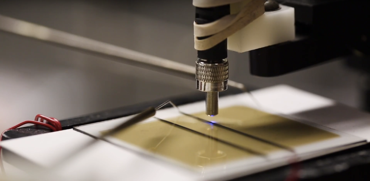
An organic solar cell testing inside the Randall Lab on Central Campus Ann Arbor, MI. University of Michigan researchers have found a way to coax electrons to travel much further than was previously thought possible in the materials often used for organic solar cells and other organic semiconductors. Unlike the inorganic solar cells widely used today, organics can be made of inexpensive, flexible carbon-based materials like plastic. Manufacturers could churn out rolls of them in a variety of colors and configurations, to be laminated unobtrusively into almost any surface. Credit: Robert Coelius/Michigan Engineering, Communication and Marketing
In an advance that could push cheap, ubiquitous solar power closer to reality, University of Michigan researchers have found a way to coax electrons to travel much further than was previously thought possible in the materials often used for organic solar cells and other organic semiconductors.
“For years, people had treated the poor conductivity of organics as an unavoidable fact, and this shows that that’s not always the case,” said Stephen Forrest, the Peter A. Franken Distinguished University Professor of Engineering and Paul G. Goebel Professor of Engineering at U-M, who led the research.
Unlike the inorganic solar cells widely used today, organics can be made of inexpensive, flexible carbon-based materials like plastic. Manufacturers could churn out rolls of them in a variety of colors and configurations, to be laminated unobtrusively into almost any surface.
Organics’ notoriously poor conductivity, however, has slowed research. Forrest believes this discovery could change the game. The findings are detailed in a study published Jan. 17 in Nature.
The team showed that a thin layer of fullerene molecules—the curious round carbon molecules also called Buckyballs—can enable electrons to travel up to several centimeters from the point where they’re knocked loose by a photon. That’s a dramatic increase; in today’s organic cells, electrons can travel only a few hundred nanometers or less.
Electrons, moving from one atom to another, make up the electric current in a solar cell or electronic component. Materials like silicon, used in today’s inorganic solar cells and other semiconductors, have tightly bound atomic networks that make it easy for electrons to travel through the material.
But organic materials have much looser bonds between individual molecules, which can trap electrons. This has long been an Achilles’ heel of organics, but the new discovery shows that it may be possible to tweak their conductive properties for specific applications.
The ability to make electrons move more freely in organic semiconductors could have far-reaching implications. For example, the surface of today’s organic solar cells must be covered with a conductive electrode that collects electrons at the point where they’re initially generated. But freely moving electrons can be collected far away from their point of origination. This could enable manufacturers to shrink the conductive electrode into an invisible grid, paving the way for transparent cells that could be used on windows and other surfaces.
“This discovery essentially gives us a new knob to turn as we design organic solar cells and other organic semiconductor devices,” said Quinn Burlingame, a U-M electrical engineering and computer science graduate researcher and author on the study. “The possibility of long-range electron transport opens up a lot of new possibilities in device architecture.
Burlingame says that the initial discovery of the phenomenon came as something of an accident as the team was experimenting with organic solar cell architecture in hopes of boosting efficiency. Using a common technique called vacuum thermal evaporation, they layered in a thin film of C60 fullerenes—each made of 60 carbon atoms—on top of an organic cell’s power-producing layer, where the photons from sunlight knock electrons loose from their associated molecules. On top of the fullerenes, they put another layer to prevent the electrons from escaping.
They discovered something they’d never seen before in an organic—electrons were skittering unfettered through the material, even outside the power-generating area of the cell. Through months of experimentation, they determined that the fullerene layer formed what’s known as an energy well—a low-energy area that prevents the negatively charged electrons from recombining with the positive charges left behind in the power-producing layer.
“You can imagine an energy well as sort of a canyon—electrons fall into it and can’t get back out,” said Caleb Cobourn, a graduate researcher in the U-M Department of Physics and an author on the study. “So they continue to move freely in the fullerene layer instead of recombining in the power-producing layer, as they normally would. It’s like a massive antenna that can collect an electron charge from anywhere in the device.”
Forrest cautions that widespread use of the discovery in applications like solar cells is theoretical at this point. But, he is excited by the discovery’s larger implications for understanding and exploiting the properties of organic semiconductors.
“I believe that ubiquitous solar power is the key to powering our constantly warming and increasingly crowded planet, and that means putting solar cells on everyday objects like building facades and windows,” Forrest said. “Technology like this could help us produce power in a way that’s inexpensive and nearly invisible.”
The study is titled “Centimeter-Scale Electron Diffusion in Photoactive Organic Heterostructures.” The research was supported by the U.S. Department of Energy SunShot Program and by the Air Force Office of Scientific Research.
In the semiconductor industry, there is currently one main strategy for improving the speed and efficiency of devices: scale down the device dimensions in order to fit more transistors onto a computer chip, in accordance with Moore’s law. However, the number of transistors on a computer chip cannot exponentially increase forever, and this is motivating researchers to look for other ways to improve semiconductor technologies.
In a new study published in Nanotechnology, a team of researchers at SUNY-Polytechnic Institute in Albany, New York, has suggested that combining multiple functions in a single semiconductor device can improve device functionality and reduce fabrication complexity, thereby providing an alternative to scaling down the device’s dimensions as the only method to improve functionality.
To demonstrate, the researchers designed and fabricated a reconfigurable device that can morph into three fundamental semiconductor devices: a p-n diode (which functions as a rectifier, for converting alternating current to direct current), a MOSFET (for switching), and a bipolar junction transistor (or BJT, for current amplification).
“We are able to demonstrate the three most important semiconductor devices (p-n diode, MOSFET, and BJT) using a single reconfigurable device,” coauthor Ji Ung Lee at the SUNY-Polytechnic Institute told Phys.org. “While these devices can be fabricated individually in modern semiconductor fabrication facilities, often requiring complex integration schemes if they are to be combined, we can form a single device that can perform the functions of all three devices.”
The multifunctional device is made of two-dimensional tungsten diselenide (WSe2), a recently discovered transition metal dichalcogenide semiconductor. This class of materials is promising for electronics applications because the bandgap is tunable by controlling the thickness, and it is a direct bandgap in single layer form. The bandgap is one of the advantages of 2D transition metal dichalcogenides over graphene, which has zero bandgap.
In order to integrate multiple functions into a single device, the researchers developed a new doping technique. Since WSe2 is such a new material, until now there has been a lack of doping techniques. Through doping, the researchers could realize properties such as ambipolar conduction, which is the ability to conduct both electrons and holes under different conditions. The doping technique also means that all three of the functionalities are surface-conducting devices, which offers a single, straightforward way of evaluating their performance.
“Instead of using traditional semiconductor fabrication techniques that can only form fixed devices, we use gates to dope,” Lee said. “These gates can dynamically change which carriers (electrons or holes) flow through the semiconductor. This ability to change allows the reconfigurable device to perform multiple functions.
“In addition to implementing these devices, the reconfigurable device can potentially implement certain logic functions more compactly and efficiently. This is because adding gates, as we have done, can save overall area and enable more efficient computing.”
In the future, the researchers plan to further investigate the applications of these multifunctional devices.
“We hope to build complex computer circuits with fewer device elements than those using the current semiconductor fabrication process,” Lee said. “This will demonstrate the scalability of our device for the post-CMOS era.”
More information:
Prathamesh Dhakras, Pratik Agnihotri, and Ji Ung Lee. “Three fundamental devices in one: a reconfigurable multifunctional device in two-dimensional WSe2.” Nanotechnology. DOI: 10.1088/1361-6528/aa7350
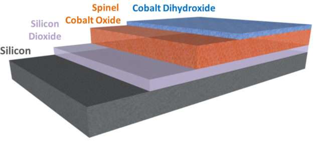
Schematic of the multi-functional water splitting catalyst layer engineered using atomic layer deposition for integration with a high-efficiency silicon cell. Credit: Ian Sharp/Berkeley Lab
Scientists have found a way to engineer the atomic-scale chemical properties of a water-splitting catalyst for integration with a solar cell, and the result is a big boost to the stability and efficiency of artificial photosynthesis.
Led by researchers at the Department of Energy’s Lawrence Berkeley National Laboratory (Berkeley Lab), the project is described in a paper published this week in the journal Nature Materials.
The research comes out of the Joint Center for Artificial Photosynthesis (JCAP), a DOE Energy Innovation Hub established in 2010 to develop a cost-effective method of turning sunlight, water, and carbon dioxide into fuel. JCAP is led by the California Institute of Technology with Berkeley Lab as a major partner.
The goal of this study was to strike a careful balance between the contradictory needs for efficient energy conversion and chemically sensitive electronic components to develop a viable system of artificial photosynthesis to generate clean fuel.
Striking the right balance
“In order for an artificial photosystem to be viable, we need to be able to make it once, deploy it, and have it last for 20 or more years without repairing it,” said study principal investigator Ian Sharp, head of materials integration and interface science research at JCAP.
The problem is that the active chemical environments needed for artificial photosynthesis are damaging to the semiconductors used to capture solar energy and power the device.
“Good protection layers are dense and chemically inactive. That is completely at odds with the characteristics of an efficient catalyst, which helps to split water to store the energy of light in chemical bonds,” said Sharp, who is also a staff scientist at Berkeley Lab’s Chemical Sciences Division. “The most efficient catalysts tend to be permeable and easily transform from one phase to another. These types of materials would usually be considered poor choices for protecting electronic components.”
By engineering an atomically precise film so that it can support chemical reactions without damaging sensitive semiconductors, the researchers managed to satisfy contradictory needs for artificial photosystems.
“This gets into the key aspects of our work,” said study lead author Jinhui Yang, who conducted the work as a postdoctoral researcher at JCAP. “We set out to turn the catalyst into a protective coating that balances these competing properties.”
Jinhui Yang performing X-ray photoelectron spectroscopy measurements, which are used to understand the chemical properties of surfaces, at the Joint Center for Artificial Photosynthesis. Credit: Robert Paz/Caltech
Doing double duty
The researchers knew they needed a catalyst that could not only support active and efficient chemical reactions, but one that could also provide a stable interface with the semiconductor, allow the charge generated by the absorption of light from the semiconductor to be efficiently transferred to the sites doing catalysis, and permit as much light as possible to pass through.
They turned to a manufacturing technique called plasma-enhanced atomic layer deposition, performed at the Molecular Foundry at Berkeley Lab. This type of thin-film deposition is used in the semiconductor industry to manufacture integrated circuits.
“This technique gave us the level of precision we needed to create the composite film,” said Yang. “We were able to engineer a very thin layer to protect the sensitive semiconductor, then atomically join another active layer to carry out the catalytic reactions, all in a single process.”
The first layer of the film consisted of a nanocrystalline form of cobalt oxide that provided a stable, physically robust interface with the light-absorbing semiconductor. The other layer was a chemically reactive material made of cobalt dihydroxide.
“The design of this composite coating was inspired by recent advances in the field that have revealed how water-splitting reactions occur, at the atomic scale, on materials. In this way, mechanistic insights guide how to make systems that have the functional properties we need,” said Sharp.
Using this configuration, the researchers could run photosystems continuously for three days—potentially longer—when such systems would normally fail in mere seconds.
“A major impact of this work is to demonstrate the value of designing catalysts for integration with semiconductors,” said Yang. “Using a combination of spectroscopic and electrochemical methods, we showed that these films can be made compact and continuous at the nanometer scale, thus minimizing parasitic light absorption when integrated on top of photoactive semiconductors.”
The study authors noted that while this is an important milestone, there are many more steps needed before a commercially viable artificial photosystem is ready for deployment.
“In general, we need to know more about how these systems fail so we can identify areas to target for future improvement,” said Sharp. “Understanding degradation is an important avenue to making something that is stable for decades.”
More information: Jinhui Yang et al. A multifunctional biphasic water splitting catalyst tailored for integration with high-performance semiconductor photoanodes, Nature Materials (2016). DOI: 10.1038/nmat4794
Check out our Flipboard magazineESISTIf you enjoy reading our posts. All of our handpicked articles will be delivered to the flipboard magazine every day.